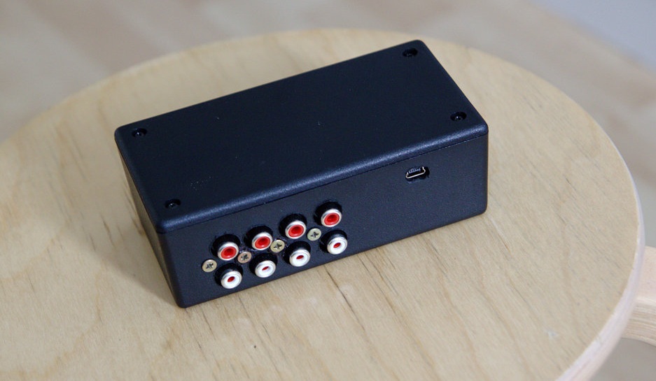
Building a USB audio DAC looks deceptively simple on a block diagram. USB data goes in, music comes out, and somewhere in the middle a tiny silicon wizard converts numbers into voltage. Easy, right? Unfortunately, the electrons have read the datasheets, and they know exactly where you cut corners.
A genuinely high-performance USB DAC is not created merely by buying the converter chip with the most heroic number of bits printed on its product page. The final sound and measured performance depend on the USB interface, clock architecture, power supplies, grounding, current-to-voltage conversion, output filtering, PCB layout, firmware, enclosure, and even the way the finished board is tested.
The classic DIY project behind this concept combined a Texas Instruments PCM2707C USB interface, a PCM1794A audio DAC, and an OPA4134 audio operational amplifier. It was an ambitious and educational design, especially for a home-etched, single-sided board. Today, the same architecture remains useful as a teaching tool, although a modern builder may choose a newer USB Audio Class 2 interface, improved regulators, a multilayer PCB, and a carefully measured analog stage.
What “High-End” Should Mean
The term high-end audio has occasionally been used to sell everything from carefully engineered electronics to cables apparently blessed during a full moon. For a DIY USB audio DAC, it is better to define the term with practical goals:
- Reliable, driver-compatible USB operation
- Bit-perfect transfer at the intended sample rates
- Low clock jitter and sensible clock distribution
- Low output noise, hum, and harmonic distortion
- Accurate channel balance and frequency response
- A stable analog output capable of driving the intended load
- No pops, clicks, crashes, or mysterious smoke signals
A design that plays 32-bit, 768-kHz files but hums whenever a laptop charger is connected is not high-end. It is merely very enthusiastic.
The Basic USB DAC Signal Chain
A practical USB DAC can be divided into six major sections:
- USB connector, protection, and interface controller
- Audio clock generation and distribution
- I2S or another serial-audio connection
- Digital-to-analog converter
- Current-to-voltage conversion, filtering, and buffering
- Power supplies, grounding, and physical construction
Each section can limit the performance of everything after it. Installing a superb DAC chip behind a noisy USB receiver is like hiring a concert pianist and giving them a piano with three loose legs.
Starting with the Classic Architecture
The PCM2707C USB Interface
The PCM2707C is a convenient all-in-one USB audio device. It handles USB communication without custom application firmware and can output 16-bit I2S audio at 32, 44.1, or 48 kHz. That is sufficient for CD-quality playback and remains perfectly usable for many listening systems.
Its limitation is obvious in a modern design: connecting a 24-bit, 192-kHz DAC downstream does not magically turn a 16-bit, 48-kHz USB stream into high-resolution audio. The DAC can only convert the samples it receives. The original combination therefore offered an excellent analog converter and output stage, but the USB receiver established the maximum incoming resolution.
This does not make the design pointless. A well-implemented 16-bit system can outperform a poorly designed high-resolution product. It does mean that a new build should choose its USB interface according to its real requirements rather than the size of the sample-rate badge planned for the front panel.
The PCM1794A Converter
The PCM1794A is a differential-current-output stereo DAC designed for high-performance audio. It accepts common serial-audio formats, supports sampling rates into the high-resolution range, and offers strong dynamic-range and distortion specifications when implemented correctly.
The important phrase is “when implemented correctly.” Its outputs are currents rather than ready-to-use line-level voltages. The surrounding analog circuitry must convert those currents into voltage, remove unwanted high-frequency energy, combine or preserve the differential outputs, and provide enough drive for the next device.
The OPA4134 Analog Stage
The OPA4134 is a quad FET-input operational amplifier intended for demanding audio applications. In the classic DAC design, its four amplifier sections can serve the left and right current-to-voltage stages and subsequent differential or low-pass filtering functions.
It is still a respectable part, but it should not be selected solely because it has the word “audio” in its description. A modern design can also evaluate newer low-noise op amps. The best choice depends on source current, feedback resistance, required output swing, supply rails, stability, load capacitance, voltage noise, current noise, and circuit topology.
Choosing a Modern USB Audio Interface
For a new high-end USB audio DAC, a USB Audio Class 2 implementation is usually more flexible than the older full-speed approach. Modern interface platforms can support asynchronous transfer, 24- or 32-bit sample containers, multiple clock families, and sample rates up to 192 or 384 kHz, depending on firmware and hardware.
XMOS devices are common in commercial and DIY projects because reference software is available for USB Audio Class operation, I2S output, clock control, device descriptors, and optional features such as MIDI, S/PDIF, or firmware updates. Microcontrollers with high-speed USB and suitable audio peripherals are another option, although firmware complexity increases quickly.
Before choosing an interface, define the product instead of shopping by acronym:
- Is stereo playback enough?
- Are recording inputs required?
- Which sample rates must be supported?
- Is DSD genuinely needed?
- Will the DAC be bus-powered or self-powered?
- Are physical volume controls or remote functions required?
- Which operating systems must be tested?
Every added feature creates more firmware states, clock combinations, power conditions, and opportunities for a computer to greet the device with the digital equivalent of a blank stare.
Asynchronous USB and Clocking
In an asynchronous USB audio design, the DAC side controls the audio timing and tells the host how quickly to deliver data. This allows the audio conversion clock to be derived from local oscillators rather than following the timing of incoming USB packets directly.
A common design uses separate low-jitter oscillators for the 44.1-kHz and 48-kHz sample-rate families. The 44.1-kHz family includes rates such as 44.1, 88.2, and 176.4 kHz, while the 48-kHz family includes 48, 96, and 192 kHz. Firmware or clock-selection logic activates the appropriate oscillator.
Clock traces should be short, clean, and routed away from high-impedance analog nodes. Avoid creating unnecessary branches. Provide proper local decoupling for oscillators and clock buffers, and check signal edges with an oscilloscope rather than assuming that a square wave drawn in the schematic will remain square after touring the PCB.
Clock jitter matters, but it should be treated as an engineering parameter, not a supernatural force. Use appropriate oscillators, good power, correct termination where needed, and a DAC architecture with sensible jitter tolerance. Then measure the output for jitter-related sidebands instead of arguing about adjective density.
Power Supply Design: Where Good DACs Go to Suffer
A USB cable provides data and power, but bus power may contain switching noise, processor activity, and ground disturbances from the host computer. Feeding it directly into every sensitive section is convenient, but convenience is not the same thing as performance.
Separate the Power Domains
A high-performance design normally treats the following as distinct loads:
- USB transceiver and digital interface logic
- Audio clocks
- DAC digital supply
- DAC analog supply
- Voltage-reference or common-mode circuitry
- Operational-amplifier rails
- Optional headphone-amplifier supply
That does not mean each pin needs its own transformer and emotional-support regulator. It means noisy and sensitive sections should not be thoughtlessly chained to the same high-impedance supply path.
Switching Regulators and LDOs
Switching converters are efficient and useful when generating required voltages from USB or an external adapter. Their outputs can then feed low-noise linear regulators for sensitive clocks and analog circuitry. The switching frequency, layout, inductor current loop, output filter, regulator stability, thermal behavior, and load transients all deserve attention.
Place ceramic bypass capacitors close to each supply pin, with short connections to the appropriate ground plane. Larger local capacitors can supply lower-frequency current demands. Follow the regulator and converter datasheets instead of assembling a random capacitor buffet and hoping every value becomes friends.
USB Isolation
Galvanic isolation can reduce ground-loop problems and prevent host-side noise from flowing directly into the audio ground. High-speed USB isolation is now possible with dedicated components, but it adds cost, isolated power requirements, PCB area, and layout complexity.
Isolation is not automatically necessary. A self-powered DAC with a well-planned grounding system may perform beautifully without it. Include isolation when measurements or system requirements justify it, not because the word looks expensive on a feature list.
Designing the Current-to-Voltage Stage
A current-output DAC such as the PCM1794A requires an I/V converter. The op amp holds the DAC output node near its intended voltage while converting output current into a proportional voltage through the feedback network.
The feedback resistance determines gain and contributes thermal noise. The feedback capacitor influences stability and high-frequency response. Larger resistor values produce more voltage from a given current, but they also increase noise and may interact with op-amp input characteristics.
A practical high-performance stage may use two steps: a low-noise I/V conversion stage followed by differential summing and low-pass filtering. Allocating more gain to the first stage can sometimes improve total noise performance, provided the op amp retains adequate headroom and stability.
Use precision thin-film resistors where matching and noise matter. For small filter capacitors in the signal path, C0G or NP0 ceramics are attractive because their capacitance is comparatively stable with applied voltage. Avoid treating every capacitor with a gold label as automatically superior; dielectric behavior and circuit position matter more than decorative typography.
Output Filtering and Buffering
Delta-sigma DACs move much of their quantization noise above the audible band. Although listeners cannot directly hear ultrasonic noise, downstream amplifiers, analog-to-digital converters, measurement equipment, or Class-D stages may react badly to it.
A carefully designed low-pass filter reduces this out-of-band energy while preserving the audible frequency response. The cutoff frequency is often placed above 20 kHz but low enough to attenuate noise-shaped ultrasonic content. The exact topology should be calculated for the DAC, desired bandwidth, op amp, load, and measurement method.
Line outputs should be protected against capacitive cables and accidental shorts. Small series resistors can improve stability, while muting circuitry can prevent startup and shutdown thumps. If headphones must be driven, use a dedicated headphone amplifier rather than asking a delicate line-stage op amp to perform weightlifting without warming up.
PCB Layout Makes or Breaks the DAC
A two-layer board can work, and the original single-sided project is proof that determined builders can accomplish surprising things. However, a four-layer PCB makes controlled return paths, continuous ground planes, power distribution, and compact routing much easier.
Place Components by Signal Flow
Keep the USB connector and interface near one side of the board. Place the clock circuitry close to the USB controller and DAC clock inputs. Keep I2S traces short. Position the DAC near the I/V stage, and place the analog output connectors near the final buffer.
Do not route USB, clock, or switching-regulator traces through the analog output section. Keep high-current loops small. Place decoupling capacitors immediately beside the pins they serve, not in a scenic neighborhood two inches away.
Grounding Strategy
Grounding advice is frequently reduced to “split analog and digital ground,” but careless splits can force return currents to take long detours. A continuous ground plane with intelligent component placement is often safer than a moat crossed by signals whose return currents have nowhere sensible to go.
When separate analog and digital regions are required, connect them according to the converter manufacturer’s recommendations and ensure no signal crosses a plane gap without a nearby return path. Consider USB shield treatment, chassis bonding, electrostatic-discharge current, and audio connector grounding as parts of one system.
Firmware and Enumeration
The firmware must describe the device accurately to the USB host. Sample rates, channel counts, bit depths, clock sources, volume controls, endpoints, and feedback behavior must agree with the hardware.
Test enumeration after cold boots, warm restarts, cable reconnection, sleep, wake, sample-rate changes, and rapid application switching. A DAC that sounds excellent only after unplugging it twice and whispering encouragement is not ready for the living room.
Provide safe muting during clock changes or invalid data conditions. Sequence regulators and reset signals correctly. Confirm that the DAC receives valid master clock, bit clock, word clock, and data before the analog stage is unmuted.
How to Test the Finished USB DAC
Listening is valuable, but it cannot replace basic engineering measurements. Start with functional checks, then measure:
- Output level and channel balance
- Frequency response
- Noise floor and dynamic range
- THD+N at several levels and frequencies
- Intermodulation distortion
- Crosstalk
- Idle tones and power-supply spurs
- Jitter-related sidebands
- Ultrasonic output noise
- Behavior under realistic loads
Use an appropriate measurement bandwidth and filtering method. Ultrasonic noise from a delta-sigma converter can overload or confuse test equipment, producing an unfair THD+N result. Document whether measurements are unweighted, A-weighted, bandwidth-limited, or taken through an external low-pass filter.
Also test the DAC with different computers, USB ports, chargers, amplifiers, and grounded or ungrounded systems. Many problems appear only when the supposedly finished device meets another product with its own opinion about ground potential.
Common Mistakes to Avoid
- Choosing the DAC chip before defining the USB interface and output requirements
- Assuming higher sample rates guarantee better audible performance
- Using noisy supply rails for clocks or analog references
- Ignoring ultrasonic noise and reconstruction filtering
- Routing clocks beside I/V feedback components
- Adding ground splits without understanding return-current paths
- Driving headphones directly from a line output
- Skipping mute and power-sequencing circuits
- Judging performance only by listening volume
- Ordering a four-layer PCB before checking every footprint
Workshop Experience: What Building a High-End USB Audio DAC Teaches
The most useful experience from a project like this is discovering that the schematic is only the beginning. On paper, the system may contain a USB controller, two oscillators, a DAC, a few op amps, and several regulators. On the bench, it becomes a small ecosystem in which every section is capable of irritating every other section.
The first milestone is usually USB enumeration. Seeing the device name appear on a computer feels like victory, even though no useful audio may exist yet. At this stage, descriptor errors, incorrect endpoint sizes, bad oscillator configuration, and reset timing can make the device appear intermittently or connect at the wrong speed. The lesson is to test the digital interface independently before debugging the analog stage.
The next surprise often arrives when I2S is examined. A casual continuity check may show that all traces are connected, yet the word clock is inverted, data alignment is wrong, or the DAC expects a different bit depth. A logic analyzer quickly becomes more valuable than a collection of premium resistors. Once master clock, bit clock, left-right clock, and data are verified, a large portion of the mystery disappears.
Power-supply debugging tends to be less theatrical but more important. A regulator may show the correct voltage on a multimeter while carrying high-frequency switching residue that appears plainly on an oscilloscope. Moving a bypass capacitor, reducing the area of a switching-current loop, or isolating an oscillator rail can improve the output spectrum more than replacing the DAC chip with a more expensive model.
The analog stage brings its own character-building exercise. An I/V converter that works in simulation may oscillate when connected to a real DAC, real PCB traces, and real test leads. Excessive ringing, hot op amps, unexplained noise, or different behavior between channels usually points toward stability, grounding, or component-placement problems rather than defective music files. Short feedback loops and carefully selected capacitor values become much more persuasive after an op amp has attempted to broadcast at several megahertz.
Enclosure work also matters. A bare board can measure well on an isolated bench and develop hum after being installed in a metal case. The USB shield, chassis, analog ground, power-entry ground, and RCA connector shells must be considered together. Insulated connectors or a deliberate chassis bond can solve a problem that no amount of firmware rewriting will touch.
Listening tests are most useful after measurements confirm that both channels are behaving normally. Level-matched comparisons help prevent a slightly louder output from being mistaken for wider soundstage, deeper emotion, or improved lunar alignment. Good engineering does not remove the pleasure of listening; it removes avoidable reasons for fooling oneself.
The final lesson is that “high-end” is not a particular DAC chip, sample rate, capacitor brand, or aluminum knob. It is the cumulative result of sensible architecture, clean power, controlled clocks, stable analog circuitry, careful layout, robust firmware, repeatable measurements, and patient debugging. When all of those pieces work together, the completed USB audio DAC becomes more than a box that converts data into voltage. It becomes a quiet, reliable instrument that lets the recording speak without the circuit constantly interrupting.
Note: Verify component status, package dimensions, electrical limits, regulator stability requirements, and the latest manufacturer datasheets before ordering parts or fabricating the PCB.